- 您现在的位置:买卖IC网 > Sheet目录308 > ADUM5230ARWZ-RL (Analog Devices Inc)IC ISOLATOR 2CH HBRIDGE 16-SOIC
�� ��
��
��ADuM5230�
�APPLICATIONS� INFORMATION�
�Data� Sheet�
�THEORY� OF� OPERATION�
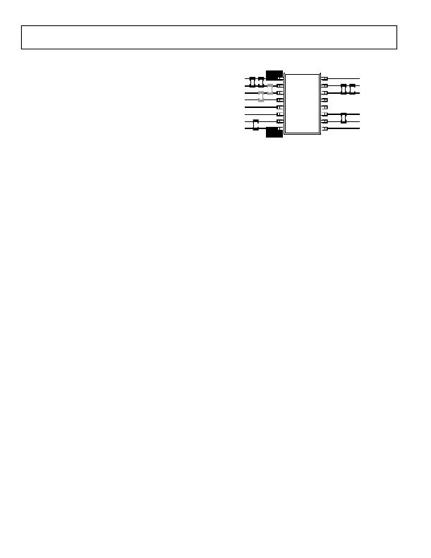
�GND� 1�
�V� OA�
�The� dc-to-dc� converter� section� of� the� ADuM5230� works� on�
�principles� that� are� common� to� most� modern� power� supply�
�designs.� It� is� implemented� as� an� open-loop� PWM� controller,�
�which� sets� the� power� level� being� transferred� to� the� secondary.�
�V� DD1� power� is� supplied� to� an� oscillating� circuit� that� switches�
�current� into� a� chip-scale� air� core� transformer.� On� the� secondary�
�V� DD1�
�V� ADJ�
�GND� 1�
�V� IA�
�V� IB�
�V� DD1�
�GND� 1�
�ADuM5230�
�TOP� VIEW�
�(Not� to� Scale)�
�V� ISO�
�GND� ISO�
�DNC�
�DNC�
�GND� B�
�V� DDB�
�V� OB�
�side,� power� is� rectified� to� a� dc� voltage.� The� voltage� is� then�
�clamped� to� approximately� 18� V� and� provided� to� the� secondary�
�side� V� OA� data� channel� and� to� the� V� ISO� pin� for� external� use.� The�
�output� voltage� is� unregulated� and� varies� with� load.�
�The� PWM� duty� cycle� is� set� by� internal� bias� elements,� but� can�
�be� controlled� externally� through� the� V� ADJ� pin� with� an� external�
�resistor� network.� This� feature� allows� the� user� to� boost� the�
�available� power� at� the� secondary,� or� reduce� excess� power� if� it� is�
�not� required� for� the� application� (see� the� Power� Consumption�
�section).�
�Undervoltage� lockouts� are� provided� on� the� V� DD1� ,� V� DDB� ,� and� V� ISO�
�supply� lines� to� interlock� the� data� channels� from� low� supply�
�voltages.�
�PC� BOARD� LAYOUT�
�The� ADuM5230� digital� isolator� with� a� 150� mW� iso� Power?�
�integrated� dc-to-dc� converter� requires� no� external� interface�
�circuitry� for� the� logic� interfaces.� Power� supply� bypassing� is�
�required� at� the� input� and� output� supply� pins� (see� Figure� 15).�
�The� power� supply� section� of� the� ADuM5230� uses� a� very� high�
�oscillator� frequency� to� pass� power� efficiently� through� its� chip�
�scale� transformers.� In� addition,� the� normal� operation� of� the�
�data� section� of� the� i� Coupler?� introduces� switching� transients� on�
�the� power� supply� pins.� Bypass� capacitors� are� required� for�
�several� operating� frequencies.� Noise� suppression� requires� a� low�
�inductance� high� frequency� capacitor;� ripple� suppression� and�
�proper� regulation� require� a� large� value� capacitor.� These� are� most�
�conveniently� connected� between� Pin� 1� and� Pin� 2� for� V� DD1� and�
�between� Pin� 15� and� Pin� 14� for� V� ISO� .� To� suppress� noise� and�
�reduce� ripple,� a� parallel� combination� of� at� least� two� capacitors� is�
�required.� The� recommended� capacitor� values� are� 0.1� μF� and�
�10� μF.� It� is� strongly� recommended� that� a� very� low� inductance�
�ceramic� or� equivalent� capacitor� be� used� for� the� smaller� value.�
�The� total� lead� length� between� both� ends� of� the� capacitor� and�
�the� input� power� supply� pin� should� not� exceed� 20� mm.�
�Bypassing� with� noise� suppression� and� stiffening� capacitors� is�
�recommended� between� Pin� 1� and� Pin� 2,� a� bypass� capacitor� is�
�recommended� between� Pin� 7� and� Pin� 8.� Bypassing� with� noise�
�suppression� and� stiffening� capacitors� is� recommended� between�
�Pin� 14� and� Pin� 15.�
�See� the� AN-0971� Application� Note� for� board� layout� guidelines�
�and� reduction� of� radiated� emissions.�
�DNC� =� DO� NOT� CONNECT�
�Figure� 15.� Recommended� Printed� Circuit� Board� Layout�
�In� applications� involving� high� common-mode� transients,� care�
�should� be� taken� to� ensure� that� board� coupling� across� the� isolation�
�barrier� is� minimized.� Furthermore,� the� board� layout� should� be�
�designed� such� that� any� coupling� that� does� occur� equally� affects�
�all� pins� on� a� given� component� side.� Failure� to� ensure� this� may�
�cause� voltage� differentials� between� pins� exceeding� the� absolute�
�maximum� ratings� specified� in� Table� 6,� leading� to� latch-up�
�and/or� permanent� damage.�
�The� ADuM5230� is� a� power� device� that� dissipates� about� 1� W� of�
�power� when� fully� loaded� and� run� at� maximum� speed.� Because� it�
�is� not� possible� to� apply� a� heat� sink� to� an� isolation� device,� the� device�
�primarily� depends� on� heat� dissipation� into� the� PCB� through� the�
�GND� pins.� If� the� device� is� used� at� high� ambient� temperatures,�
�care� should� be� taken� to� provide� a� thermal� path� from� the� GND�
�pins� to� the� PCB� ground� plane.� The� board� layout� in� Figure� 15�
�shows� enlarged� pads� for� Pin� 1� and� Pin� 8.� Multiple� vias� should�
�be� implemented� from� the� pad� to� the� ground� plane.� This� signifi-�
�cantly� reduces� the� temperatures� inside� the� chip.� The� dimensions�
�of� the� expanded� pads� are� left� to� the� discretion� of� the� designer�
�and� the� available� board� space.�
�THERMAL� ANALYSIS�
�The� ADuM5230� part� consists� of� several� internal� die� attached� to�
�three� lead� frames,� each� with� a� die� attach� paddle.� For� the� purposes�
�of� thermal� analysis,� the� device� is� treated� as� a� thermal� unit� with�
�the� highest� junction� temperature� reflected� in� the� θ� JA� parameter�
�shown� in� Table� 2.� The� value� of� θ� JA� is� based� on� measurements�
�taken� with� the� part� mounted� on� a� JEDEC� standard� four-layer�
�board� with� fine� width� traces� and� still� air.� Under� normal� operating�
�conditions,� the� ADuM5230� operates� at� full� load� across� the� full�
�temperature� range� without� derating� the� output� current.� However,�
�following� the� recommendations� in� the� PC� Board� Layout� section�
�decreases� the� thermal� resistance� to� the� PCB,� allowing� increased�
�thermal� margin� in� high� ambient� temperatures.�
�Under� output� short-circuit� conditions,� as� shown� in� Figure� 12,�
�the� package� power� dissipation� is� within� safe� operating� limits;�
�however,� if� the� load� is� in� the� 100� Ω� range,� power� dissipation� is�
�high� enough� to� cause� thermal� damage� when� the� ambient� tempera-�
�ture� is� above� 80°C.� Care� should� be� taken� to� avoid� excessive�
�nonshort� loads� if� the� part� is� to� be� operated� at� high� temperatures.�
�Rev.� B� |� Page� 10� of� 16�
�发布紧急采购,3分钟左右您将得到回复。
相关PDF资料
ADUM5240ARZ-RL7
IC ISOLATOR 2CH W/CONV 8-SOIC
ADUM5400CRWZ-RL
IC ISOLATOR 4CH DCDC CONV 16SOIC
ADUM5402WCRWZ
IC ISOLATOR 4CH DCDC CONV 16SOIC
ADUM5404CRWZ
IC ISOLATOR 4CH DCDC CONV 16SOIC
ADUM6132ARWZ-RL
IC GATE DRIVER ISOLATED 16-SOIC
ADUM6201CRIZ
ISOLATED DC-DC CONV 2CH 16SOIC
ADUM6404ARWZ
IC ISOLATOR 4CH DCDC CONV 16SOIC
ADUM7241CRZ-RL7
ISOLATOR DGTL 1KVRMS 2CH 8SOIC
相关代理商/技术参数
ADUM5230WARWZ
功能描述:Gate Driver Magnetic Coupling 2500Vrms 2 Channel 16-SOIC 制造商:analog devices inc. 系列:iCoupler? 包装:管件 零件状态:有效 技术:磁耦合 通道数:2 电压 - 隔离:2500Vrms 共模瞬态抗扰度(最小值):25kV/μs 传播延迟 tpLH / tpHL(最大值):100ns,100ns 脉宽失真(最大):8ns 上升/下降时间(典型值):25ns,10ns(最大) 电流 - 输出高,低:- 电流 - 峰值输出:- 电压 - 正向(Vf)(典型值):- 电流 - DC 正向(If):- 电压 - 电源:12 V ~ 18.5 V 工作温度:-40°C ~ 105°C 安装类型:表面贴装 封装/外壳:16-SOIC(0.295",7.50mm 宽) 供应商器件封装:16-SOIC 认可:UR 标准包装:47
ADUM5230WARWZ-RL
功能描述:Gate Driver Magnetic Coupling 2500Vrms 2 Channel 16-SOIC 制造商:analog devices inc. 系列:iCoupler? 包装:带卷(TR) 零件状态:有效 技术:磁耦合 通道数:2 电压 - 隔离:2500Vrms 共模瞬态抗扰度(最小值):25kV/μs 传播延迟 tpLH / tpHL(最大值):100ns,100ns 脉宽失真(最大):8ns 上升/下降时间(典型值):25ns,10ns(最大) 电流 - 输出高,低:- 电流 - 峰值输出:- 电压 - 正向(Vf)(典型值):- 电流 - DC 正向(If):- 电压 - 电源:12 V ~ 18.5 V 工作温度:-40°C ~ 105°C 安装类型:表面贴装 封装/外壳:16-SOIC(0.295",7.50mm 宽) 供应商器件封装:16-SOIC 认可:UR 标准包装:1,000
ADUM5240
制造商:AD 制造商全称:Analog Devices 功能描述:Dual-Channel Isolators with Integrated DC/DC Converter, 50 mW
ADUM5240_12
制造商:AD 制造商全称:Analog Devices 功能描述:Dual-Channel Isolators with isoPower Integrated DC-to-DC Converter, 50 mW
ADUM5240ARZ
功能描述:IC ISOLATOR 2CH W/CONV 8-SOIC RoHS:是 类别:隔离器 >> 数字隔离器 系列:IsoPower®, iCoupler® 标准包装:66 系列:iCoupler® 输入 - 1 侧/2 侧:2/2 通道数:4 电源电压:3.3V,5V 电压 - 隔离:2500Vrms 数据速率:25Mbps 传输延迟:60ns 输出类型:逻辑 封装/外壳:20-SSOP(0.209",5.30mm 宽) 供应商设备封装:20-SSOP 包装:管件 工作温度:-40°C ~ 105°C
ADUM5240ARZ-RL7
功能描述:IC ISOLATOR 2CH W/CONV 8-SOIC RoHS:是 类别:隔离器 >> 数字隔离器 系列:IsoPower®, iCoupler® 产品培训模块:IsoLoop® Isolator 标准包装:50 系列:IsoLoop® 输入 - 1 侧/2 侧:5/0 通道数:5 电源电压:3 V ~ 5.5 V 电压 - 隔离:2500Vrms 数据速率:110Mbps 传输延迟:12ns 输出类型:CMOS 封装/外壳:16-SOIC(0.154",3.90mm 宽) 供应商设备封装:16-SOIC N 包装:管件 工作温度:-40°C ~ 85°C 其它名称:390-1053-5
ADUM5240BRZ
制造商:Analog Devices 功能描述:DGTL ISOLATORS 8SOIC - Rail/Tube
ADUM5240XRZ
制造商:Analog Devices 功能描述:DUAL-CHANNEL ISOLATORS WITH INTEGRATED DC/DC CONVERTER - Rail/Tube